
matosicv0.0.0.10
2026-05-25
Castellation bridges, a dead reset button, and what v0.0.0.18 has to fix.
Three days after the first v0.0.0.17 board ran QMK end-to-end, I sat down to bring up the second one. Two hours later I had nine LEDs glowing, one working switch out of nine, and a XIAO whose reset button I had cooked with a heat gun. The board #2 build was a masterclass in everything the current PCB asks too much of a human soldering iron. This is the story of fighting the same castellation pad for four rounds of solder wick, and the four design changes v0.0.0.18 needs so the next maker (or the next me) doesn't fight it again.
The setup: a fresh XIAO and a fresh PCB
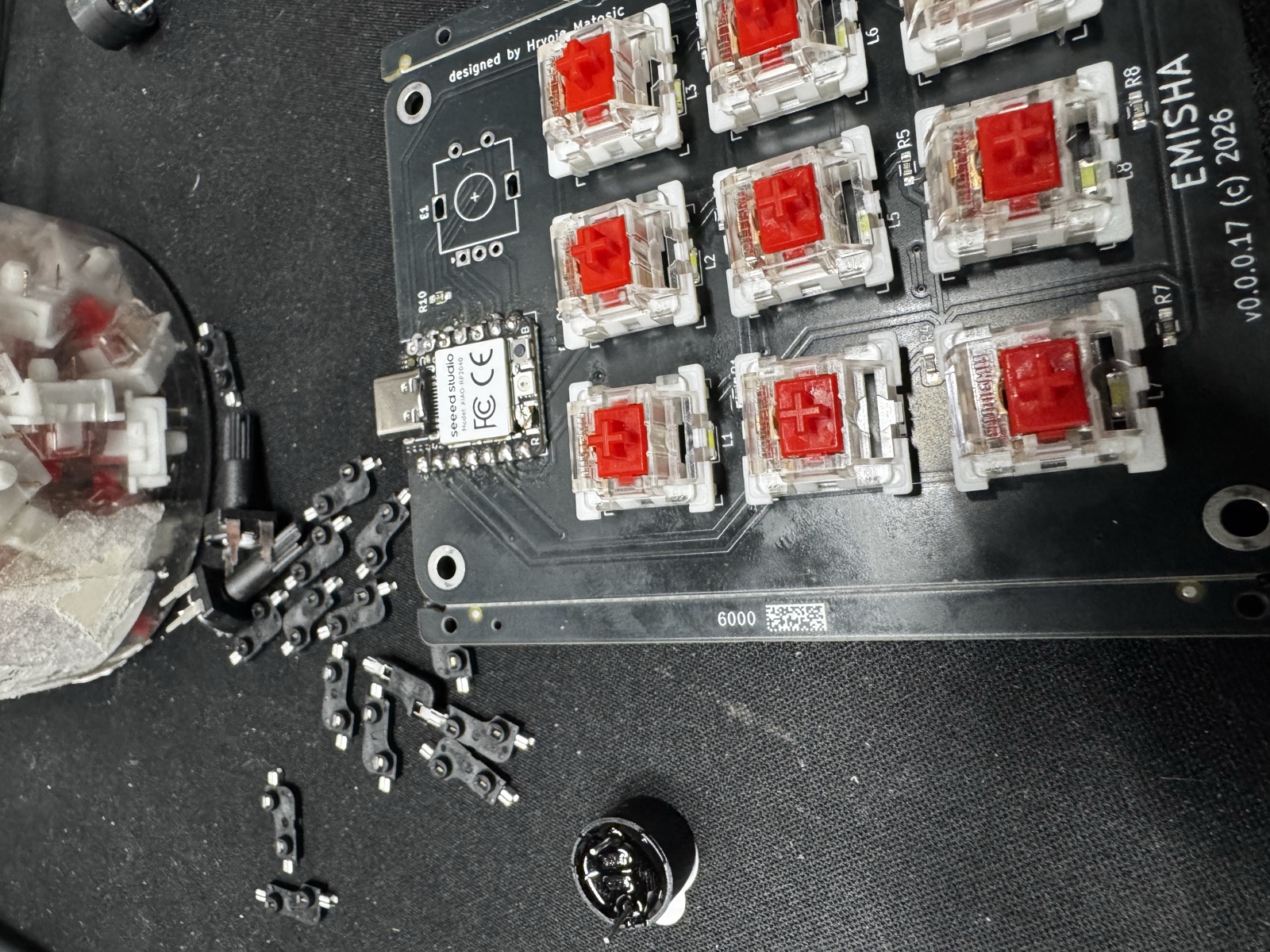
v0.0.0.17 is a XIAO module socket design. The Seeeduino XIAO RP2040 is a 14-pin castellated module with USB-C, BOOT and RESET buttons, and a hand- solderable 21 mm × 17.8 mm footprint. The macropad PCB has pads laid out to take the XIAO in “flush mount” orientation — you lay the module flat onto the host PCB and solder each castellation pad to the matching pad underneath. That's how board #1 was assembled, the one I've been building firmware on for the last week. It worked first try.
Board #2 was supposed to be the same thing. New
module, new bare PCB out of the JLCPCB shipment, fresh
soldering session at my bench. I do all 14
castellations with a fine-tip iron, flood the joints
with leaded solder for confidence, plug in USB.
CIRCUITPY mounts. boot_out.txt
reports CircuitPython 10.2.1 on a Seeeduino XIAO
RP2040 with a UID. So the chip is alive and
enumerating. Good start.
The first sign of trouble
I copy over a minimal code.py that does
nothing but flip board.D0 high and low
every second. D0 is the gate signal for Q1, the
little SOT-23 NPN that switches the 5 V rail
feeding all nine backlight LEDs. If D0 toggles, all
nine LEDs should pulse in unison.
They do. Perfect synchronized blink, nine little red dots through the empty hot-swap sockets. So D0, the Q1 driver, the 470 Ω rail resistor, and the entire LED chain are alive. Power rails are fine. Castellations for 5V / GND / 3V3 must be joined. The XIAO is healthy.
Then I copy over the real firmware. CIRCUITPY auto-reloads, the serial REPL prints the macropad startup banner, and I open a text editor and start tapping switches.
One switch types. SW6 — middle row, right
column — types 6 when I press it.
The other eight do nothing at all.
One working key tells you a lot
The 9-key matrix on this PCB is wired as 3 rows × 3 columns. The firmware scans by driving each row pin LOW one at a time, then reading the three column pins; any column that reads LOW while its row is LOW is a pressed key. On the XIAO that means three row pins (D1, D2, D3) and three column pins (D4, D5, D6).
SW6 sits at matrix[1][2] — row 1,
column 2 — which on the XIAO is the
intersection of D2 driving LOW and
D6 reading LOW. So that single working
key proved D2 and D6 were alive. Every other key
failing proved one or both of its row and
column pins were not.
Two scenarios fit the symptoms:
- The XIAO is partially fried — specific GPIO pads on the chip died during reflow heat.
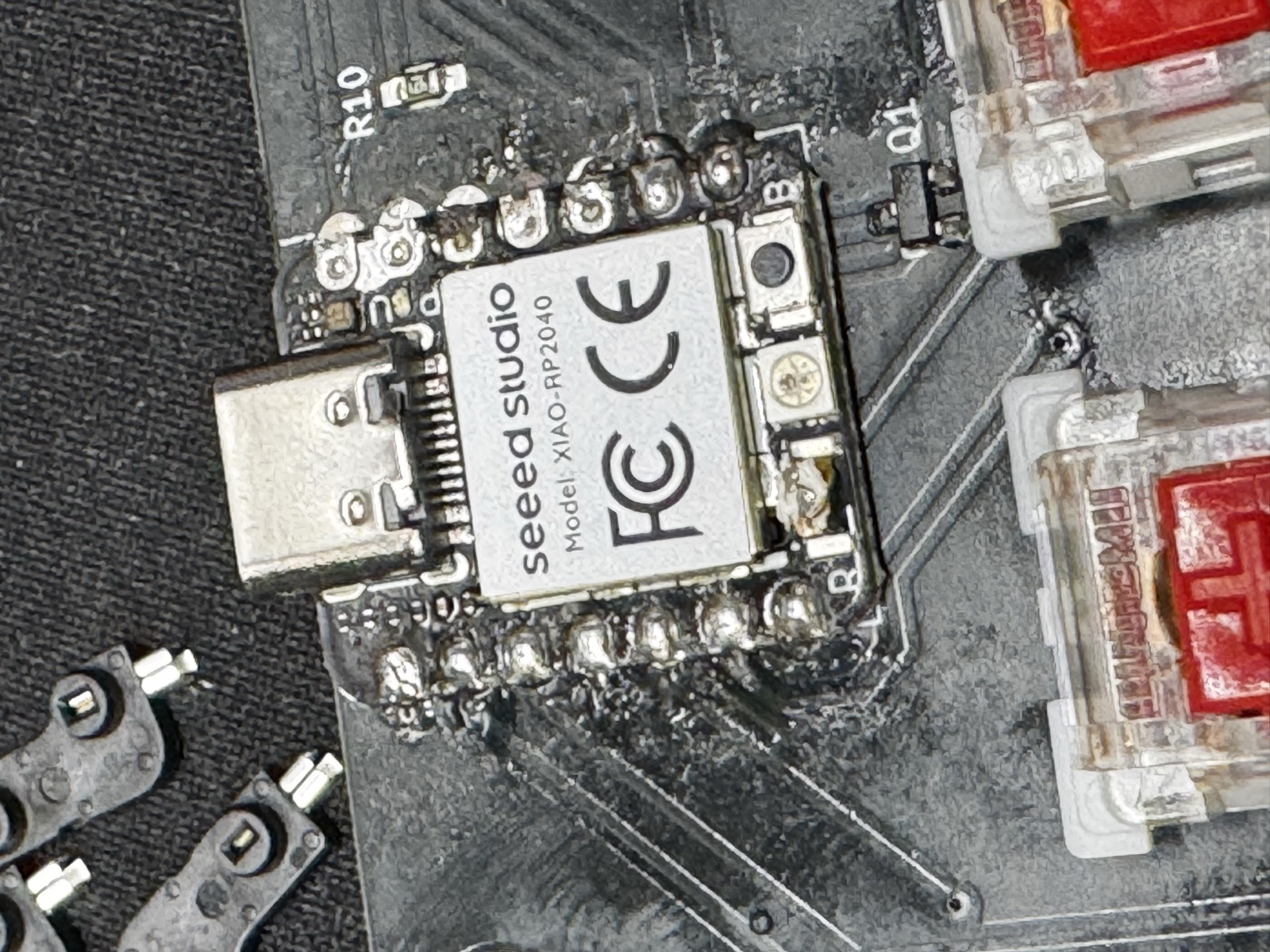
- The castellation joints for those pins are bad — either cold (no electrical contact at all) or shorted to a neighbouring pad.
A heat-damaged chip is the more dramatic answer. Solder joint problems are the boring, more likely one. The way to tell them apart is to deploy a diagnostic firmware that prints the raw matrix grid on every scan, and then methodically work the soldering iron.
The diagnostic firmware
I wrote a CircuitPython sketch whose job is to scan
the 3×3 matrix every ~50 ms and print the
state of all nine intersections to serial whenever
anything changes — idle is suppressed so the
terminal isn't a wall of H H H. Every
press of a real key shows up as an L
appearing at the right grid cell. Every dead row or
dead column shows up as an entire row or column that
stays H forever.
I press all nine switches in sequence. Only SW6 triggers a grid change. The other eight presses are invisible to the firmware. That settles it: I have four matrix pins (D1, D3, D4, D5) that aren't reporting changes when their switches are pressed. Most likely four bad joints, not four dead silicon pads.
I also note the pattern: the dead pins are exactly the ones adjacent to working pins. D2 works, D1 and D3 (which sit right next to it on the left castellation row) don't. D6 works, D5 (its neighbour on the right row) doesn't. That looks suspiciously like solder bridges between adjacent pads — the bridge clamps the “dead” pin to whatever its neighbour is doing, so it can't be independently driven LOW.
Wick, test, wick, test
The fix for a solder bridge is desoldering braid — a thin strip of woven copper that, when heated against a joint, wicks the molten solder up into the braid by capillary action. You snip off the used (now silver) end of the braid and move on. Done well, a single bridged joint becomes two clean independent pads in about three seconds.
I work down the left side of the XIAO first, hitting each of the suspect bridges between D0/D1, D1/D2, and D2/D3. Each pad gets wicked, then reflowed with a tiny amount of fresh solder so the castellation cup has just a small concave fillet bridging it to the PCB pad — not the massive convex blob I'd originally laid down. Plug in USB, run the matrix diagnostic again, press the bottom-row switches.
D1 comes back. SW7, SW8, SW9 now print
7, 8, 9. Three
more switches alive. That's progress.
I do the same on the right side for D4/D5/D6. After
the next round, D5 comes back too —
now SW5 and SW8 also work, on top of the previously-
living SW6 and SW9. Six of nine switches firing.
Three to go: SW1, SW2, SW3, all sharing the row pin
D3, and SW1 / SW4 / SW7 all sharing the
column pin D4.
Those two pins are the bottom-most castellations on their respective sides of the XIAO — the corner pads. Corners are the hardest position to solder cleanly: gravity pulls the iron tip away from them, there's less mechanical anchor than middle pads, and the soldering iron tip is wider than the gap to the next pad over, so it's easy to leave either too little solder (open joint) or too much (bridge to the second-from-bottom pad).
The heat gun mistake
By this point I'd been at the iron for an hour and was getting impatient with the iterative dance of wick, reflow, test, wick, reflow, test. I reached for a hot air rework gun — the kind used for SMT reflow — thinking I could heat the entire bottom edge of the XIAO at once, melt all the joints simultaneously, and let surface tension pull each one into a good fillet.
The hot air rework gun is the wrong tool for this. A soldering iron tip is about 1 mm wide and touches one pad at a time for two seconds. A hot air gun blows a 10 mm column of 350 °C air across the entire end of the module for as long as you hold it there. Heat conducts through the PCB substrate, the RF shield, the chip package, and the little tact switches a few millimetres away.
When I plugged the XIAO back in after the heat gun
pass, USB still enumerated and CircuitPython still
booted. But the RESET button no longer worked. I
could press it and feel the click of the dome
switch, but no reset event reached the chip. The
tact switch had cooked — either the plastic
carrier had deformed enough to permanently bridge or
permanently open the contacts, or the trace from the
switch to the RP2040's RUN pin had been
damaged in the substrate.
In firmware development, the reset button is the
single most important hardware control on the module.
It's how you enter bootloader mode (with BOOT held)
to flash new code. Without a working reset, every
firmware update means either using
microcontroller.on_next_reset() from a
REPL to enter bootloader, or physically shorting the
BOOT/RESET pads with a piece of wire. Both work but
both are friction every single deploy. Don't
point heat guns at a module that's already
soldered.
The final state
I called it for the night with four of nine switches
working — SW5, SW6, SW8, SW9, the four keys
whose row driver is D2 or D1
and whose column is D5 or D6.
The other five (SW1, SW2, SW3, SW4, SW7) are still
dead because D3 (the top-row driver) and
D4 (column 1) refused to come back
through the wick-and-reflow rounds. The two pins
blocking those five keys are both at the bottom-most
castellation corners on each side — the
hardest positions to solder cleanly, exactly where
the wick passes are slowest to converge.
In the meantime, I've ordered nine more XIAOs from a Mexican parts shop — the per-unit price collapsed at quantity, so going to nine cost barely more than going to three. The new approach for any board I assemble by hand from now on is going to be socket the next one, don't solder it directly. A 2×7 female header at 2.54 mm pitch costs under fifty cents and lets the XIAO slot in and out with zero hand-soldering on the module itself. That's what the v0.0.0.17 design was supposed to support all along — the “socket” in “XIAO module socket” was meant literally — but I'd been flush-mounting because flush mount looks tidier and saves vertical clearance. The tidiness cost me one XIAO module's reset button and an afternoon.
What v0.0.0.18 has to fix
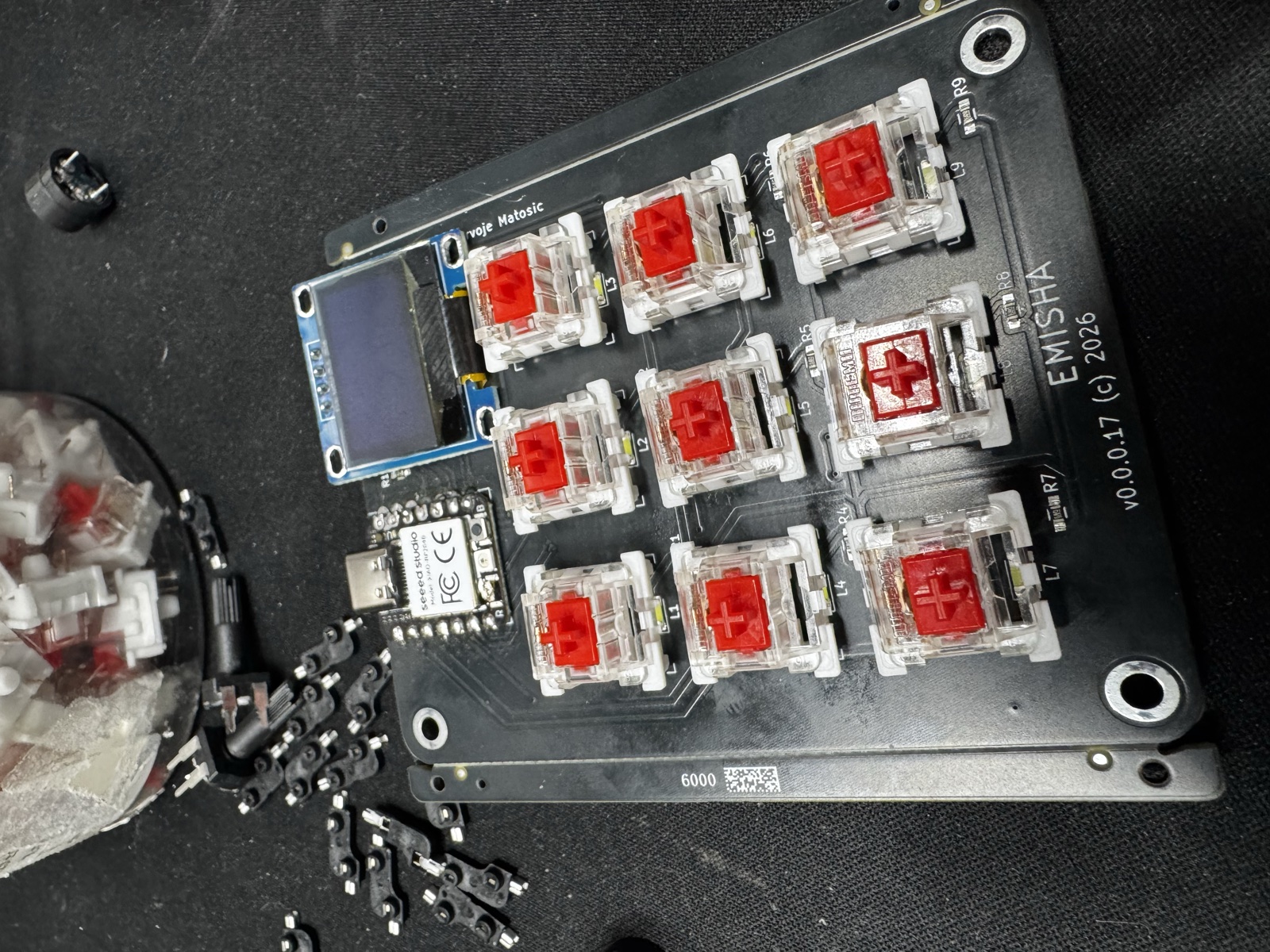
Capturing this so the next revision of the PCB makes the failure mode I just walked through structurally less likely. Four design changes for the XIAO footprint in v0.0.0.18:
Tab-shaped castellation pads. Instead of the current rectangular pads that end at the PCB edge, extend each pad inward as a wider rectangular tab. That gives the iron more landing area, makes each pad more visually distinct from its neighbour, and gives the eye an obvious target. You're trying to make a clean fillet between the castellation cup and the pad — a wider pad means there's more “right” surface area relative to the “wrong” gap between pads.
Solder mask channels between adjacent castellation pads. Right now the pads sit in shared exposed copper. Adding a thin sliver of green solder mask between every pair of adjacent pads gives molten solder a physical wall to stop at. Solder doesn't flow over solder mask, so a bridge would have to physically jump over the mask channel — far less likely than today, where the only thing stopping the bridge is the assembler's steadiness of hand.
Silkscreen orientation indicator next to the XIAO footprint. A small arrow or notch pointing toward where the USB-C connector should sit. Mounting a XIAO 180° rotated is the easiest possible footgun — the module looks symmetric — and a flipped XIAO routes 5 V to whatever pin would normally be D7. Putting the right orientation on the silk takes thirty seconds in KiCad and prevents an entire class of dead-on-arrival board.
Per-pad GPIO labels at the castellation
positions. Print D0,
D1, … GND,
5V right next to each castellation pad
so the assembler can visually confirm pin alignment
pad-by-pad before the iron ever touches the module.
Right now if you mis-aligned the XIAO by one pad
vertically (off by a single 2.54 mm step) you
might not catch it until firmware refused to enumerate.
The fifth, optional, change is to redesign the footprint so it accepts either a flush- soldered module or a 2×7 socket without the assembler having to choose at PCB-order time. That mostly comes free if you draw the castellation pads as oblong tabs that overlap a through-hole drill — flush solder goes onto the tab, the socket header goes through the hole. Some XIAO host PCBs already do this. Worth stealing.
And the harder, longer-term answer: maybe the XIAO shouldn't be on this PCB at all. The four fixes above make hand-soldering doable; the longer-term fix is to skip hand-soldering entirely. Two paths to consider for the round after v0.0.0.18: (a) keep the XIAO module and ship the next PCB to JLCPCB with the XIAO included in the PCBA so the factory does the castellation joints with real reflow, or (b) swap the XIAO out for a cheaper bare chip — an RP2040 in QFN-56, a Waveshare RP2040-Zero, or similar — and let JLCPCB SMT-place the whole thing. Either way the next bring-up doesn't start with a soldering iron. Which path wins depends on a redesign estimate I haven't done yet, but it'll be the design question for v0.0.0.19.
Why I'm publishing this
Three reasons.
One: the v0.0.0.17 PCB is open source and on GitHub. If you fork it, you're going to face this same soldering session. Better that you read this first than rediscover it the hard way with a $5 XIAO and an afternoon.
Two: hardware projects fail in public the same way they fail in private — and the failures are more useful to other people than the successes. A build log that only shows the wins is a sales page, not a journal.
Three: capturing the failure mode in writing while it's fresh means the v0.0.0.18 KiCad pass actually makes the changes above instead of vague remembering “something about castellation soldering being a problem.” The four-item list in the previous section is the spec for the next footprint revision, written down.
Next up: the new XIAO modules show up in two weeks. When they arrive I'll socket a fresh one into a new PCB instead of trying to recover the half-cooked board with more heat, draw up v0.0.0.18 with the four footprint changes above (so any future hand- build is less painful), and start the redesign estimate for the “factory-assembled module” path in parallel. Either v0.0.0.18 or v0.0.0.19 won't ship without solving the soldering problem at the design level.